
AI News
30 Aug 2026
Read 8 min
AI-assisted spectroscopic ellipsometry cuts analysis time
AI-assisted spectroscopic ellipsometry automates interpretation, cutting analysis time and boosting yields.
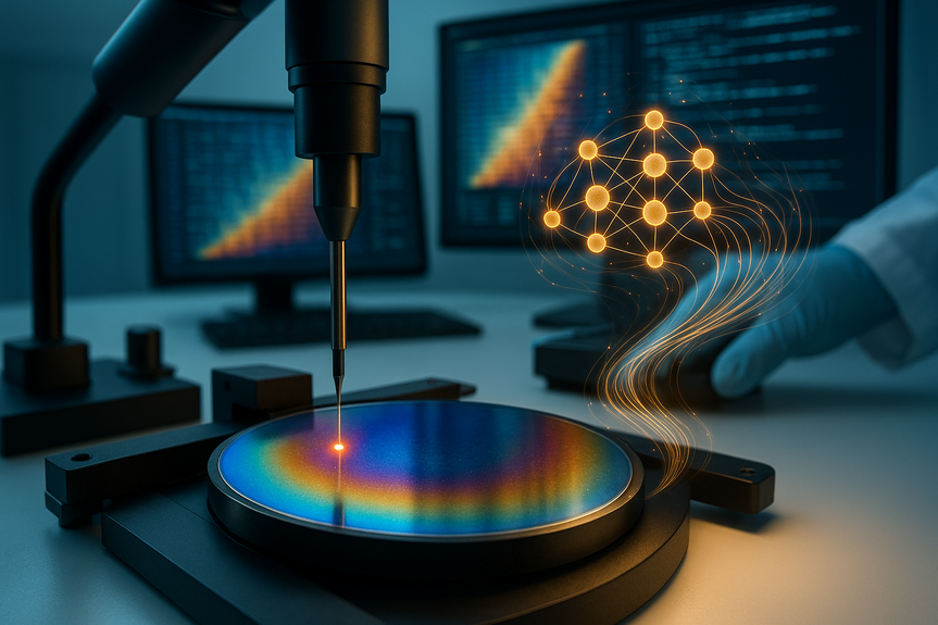
AI-assisted spectroscopic ellipsometry turns slow, expert-heavy thin-film analysis into fast, automated insight. A University of Toledo physics Ph.D. student trained neural networks on vast simulated datasets to read nonuniform layers more quickly. The result can cut a key bottleneck in solar and semiconductor lines and improve quality control without touching the product.
Nonuniform layers can stall a production line. When parts are only nanometers thick, workers cannot see problems with the naked eye. They need tools that read how light changes when it reflects from a surface. That is where spectroscopic ellipsometry shines. Now, a new AI approach aims to make this trusted method much faster and easier to use on the factory floor.
What AI-assisted spectroscopic ellipsometry means
Spectroscopic ellipsometry measures thin-film thickness and optical properties by tracking tiny changes in the polarization of light. Skilled scientists fit the measured spectra to a model of the stack. This step takes time, judgment, and many manual tweaks. AI-assisted spectroscopic ellipsometry replaces much of that manual fitting with a trained model. A neural network learns the link between spectra and film parameters across many possible real-world variations. It can then interpret new measurements more quickly, even when layers vary across a surface.Why this breakthrough matters
The bottleneck: from raw light data to decisions
– Traditional workflows require experts to adjust models again and again – Nonuniform films make fits unstable and slow – Long analysis loops delay feedback to production teams – Throughput suffers, and scrap risk risesHow AI speeds the path
– Trained networks read spectra and return thickness and optical values fast – Automated outputs improve consistency shift-to-shift – Faster analysis enables denser mapping across large panels or wafers – Inline or near-line feedback helps catch problems early Dr. Nik Podraza, professor of physics at The University of Toledo, calls this a major step for research and industry. He notes that cutting analysis time for films many times thinner than a human hair can pay off in semiconductors and energy manufacturing.From classroom to cleanroom: a student’s journey
Alex Bordovalos earned a physics bachelor’s degree in 2020 and a Professional Science Master’s in Photovoltaics in 2022 at UToledo. During an industry internship, he saw how thin-film nonuniformities slow production decisions. He leaned into his long interest in computer science and built an AI tool to accelerate ellipsometry analysis. His early results earned a first-author paper in the Journal of Applied Physics and a J.A. Woollam Outstanding Student Poster Award at the AVS International Symposium and Exhibition. He also presented at the IEEE Photovoltaic Specialists Conference.Inside the model training
Bordovalos trained the network on about half a million simulations. Each run varied expected thickness and other film properties across wide ranges, including ±50% swings. This gave the model exposure to many “messy” conditions that real devices show on a line. – Large simulated datasets cover edge cases before real data arrive – The model learns to handle irregular, nonuniform layers – Training supports materials used in thin-film solar, such as cadmium telluride (CdTe) The next step is real-world testing on cadmium telluride solar cells produced and studied at UToledo’s Wright Center for Photovoltaics Innovation and Commercialization. If results match the simulated performance, the tool can move closer to production use.Impact across solar and semiconductors
Solar manufacturing
– Map thickness across large CdTe glass panels more quickly – Link optical signatures to process drifts in near real time – Reduce rework and stabilize yieldSemiconductor fabs
– Speed metrology for ultra-thin gate oxides and dielectrics – Support uniformity checks across 200–300 mm wafers – Feed rapid data to process control loopsResearch labs
– Free scientists from repetitive fitting – Let teams scan more samples in less time – Standardize analysis across instruments and sitesWhat to watch next
– Validation: Does the AI match expert fits on real devices within tight error bounds? – Robustness: Can it handle new materials, stacks, and process shifts without retraining? – Integration: How easily does it plug into existing ellipsometers and factory software? – Governance: Clear versioning, drift checks, and human-in-the-loop review to maintain trust The University of Toledo’s strength in thin-film photovoltaics and materials science provides an ideal testbed. With cadmium telluride cells on hand and deep metrology expertise, the team can compare AI outputs to gold-standard methods and drive rapid iteration. In short, AI-assisted spectroscopic ellipsometry offers a practical way to shrink analysis time while keeping accuracy high. By moving expert knowledge into a trained model, teams can see nonuniformities sooner, adjust processes faster, and ship better products. As real-world testing progresses, expect broader adoption of AI-assisted spectroscopic ellipsometry in both research labs and advanced manufacturing lines.For more news: Click Here
FAQ
Q: What is AI-assisted spectroscopic ellipsometry?
A: AI-assisted spectroscopic ellipsometry uses trained neural networks to automate interpretation of spectroscopic ellipsometry measurements, which determine thin-film thickness and optical properties by tracking tiny changes in the polarization of reflected light. It replaces much of the manual model fitting experts perform, allowing faster and more consistent analysis of nonuniform layers.
Q: How does the AI model accelerate thin-film analysis?
A: Neural networks learn the mapping between measured spectra and film parameters from many simulated examples, so they can return thickness and optical values quickly. Automated outputs improve consistency shift-to-shift and enable denser mapping across large panels or wafers.
Q: What training data did the researcher use to build the model?
A: Alex Bordovalos trained the network on about half a million simulations that varied expected thickness and other film properties across wide ranges, including roughly ±50% swings. This large simulated dataset exposed the model to many messy, nonuniform conditions before real-world testing.
Q: Which industries and applications could benefit from AI-assisted spectroscopic ellipsometry?
A: The article highlights solar manufacturing, semiconductor fabs, and research labs as primary beneficiaries. Use cases include faster mapping of cadmium telluride (CdTe) panels, speeded metrology for ultra-thin gate oxides on 200–300 mm wafers, and freeing scientists from repetitive fitting.
Q: What validation steps remain before the AI tool can be deployed?
A: The next step is real-world testing on cadmium telluride solar cells at The University of Toledo to verify that simulated performance carries over to actual devices. The team plans to compare AI outputs against gold-standard expert fits and metrology methods to assess accuracy and readiness for production use.
Q: What technical and governance challenges does the article say need attention?
A: Key challenges include robustness to new materials, stacks, and process shifts, plus easy integration with existing ellipsometers and factory software. The article also stresses governance measures such as versioning, drift checks, and human-in-the-loop review to maintain trust and performance.
Q: Who developed this AI approach and what recognition has the work received?
A: Doctoral student Alex Bordovalos at The University of Toledo developed the neural-network approach to handle nonuniform thin films. His preliminary research appeared in the Journal of Applied Physics, earned the J.A. Woollam Outstanding Student Poster Award at the AVS symposium, and was presented at IEEE conferences.
Q: How could AI-assisted spectroscopic ellipsometry change quality control on manufacturing lines?
A: By providing faster, automated thickness and optical measurements, AI-assisted spectroscopic ellipsometry can deliver near-line or inline feedback to catch nonuniformities earlier and reduce rework. Faster analysis enables denser mapping and quicker process adjustments, which can help stabilize yield without touching the product.
Contents